
NV- 10-160(EATON)
HIGH CURRENT ION IMPLANTER SPECIFICATION
Introduction
The NV-10-160 is a high-performance ion implantation system that is capable of producing ion beams with current of up to 7 mA and energies of 20 to 160keV. The NV-10- 160 is designed for implanting semiconductor wafers in applications that require high levels of ion doping, such as pre-deposition implants, and source and drain implants.
The NV-10-160 functions basically as follows. A source material is introduced into a hot cathode type ion source, where is ionized by collisions between the source gas molecules and electrons being emitted from source filament. The source material may be either solid or gaseous. A plasma of ions and electrons forms in the arc chamber when the source material ionizes.
The ions in the plasma is extracted from the arc chamber through a slit in the chamber and emerge from the source as an ion beam that consists of several ion species. The beam then passes through an analyzer magnet, which separates the different ions in the beam by virtue of their atomic mass and charge, and allows only one ion species to continue toward the wafers.
Ion Beam Energies
· 160keV configuration : 20~160keV
Beam Current for 80kev Configuration
Beam current values are specified as measured at the disk Faraday.
|
Energy(keV) |
B11(mA) |
As75(mA) |
P31(mA) |
|
20 |
0.5 |
0.2 |
0.3 |
|
40 |
1 |
1.5 |
1 |
|
80 |
2 |
3 |
2.5 |
|
140 |
3 |
5 |
5 |
Minimum Beam Current
· 10μA
Dose Range
· 5.0E12 to 5.0E15 atoms / cm²
Mechanical Throughput
Throughput at the mechanical limit can be maintained with the implant times listed.
|
Wafer Size |
Batch Size |
Throughput |
Maximum |
|
150 |
10 |
100 |
120 |
Vacuum Performance
|
Subsystem |
Pump |
Base Pressure (Torr) |
|
Source |
Diffusion pump |
≦5.0E -06 |
|
Beamline/Resolving Housing |
Cryo Torr8 |
≦5.0E -06 |
|
Resolving Housing/Process Chamber |
Cryo Torr8 |
≦5.0E -06 |
Wafer Temperature Control
Maximum wafer temperature will not exceed 100℃ , as measured by temperature stickers shielded from direct exposure to the beam ,adhered to the front side of bare Si wafers , at all doses up to 5.0E15 atoms/cm² , for beam powers up to 1600watts (1000 watts for 125mm wafers).
Dose Control
Dose Uniformity Within A Wafer
· ≦3.0% of the mean on Si wafers for all doses between 5.0E12 to 5.0E15 atoms / cm²
· ≦4.0% of the mean on dielectric surfaces(including photoresist) for all doses between 1.0E14 and 5.0E15 atoms / cm²
Dose Repeatability/Wafer-to-Wafer and Batch-to- Batch
· ≦3.0% on bare Si wafers
· ≦4.0% on photoresist wafers
Beam Stability
· ≦ 20% beam current drift during 1hour of operation
· ≦ 30% flinches per hour at 70% of maximum beam current, 20~160keV under normal
operating conditions for singly charged B11 ,B49 ,As75 ,P31.
Charge Control Technology
· Secondary Electron Flood(SEF). The SEF provides wafer charge control through the delivery of low energy electrons to the wafer surface. Electrons from an electron gun are accelerated into a target causing emission of low energy secondary electrons. The biased extension tube improve beam neutralization and the transport of the electrons to the wafer.
Safety
Compliance
Machines designated for shipment to Europe will bear CE Mark and declaration upon customer request CE Mark includes the machinery ,Low Voltage ,and Electromagnetic Compatibility Directives.
X-Ray Emission
· ≦ 0.6μSievert / hr (60μrem / hr) at 150mm from all machine surfaces.
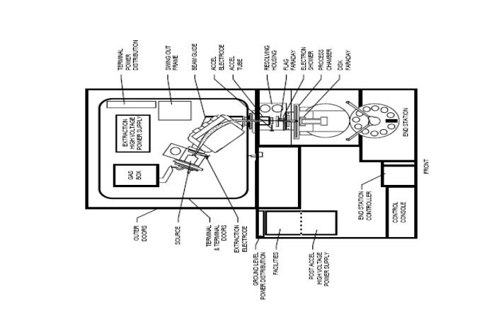
System Layout
NV- 10-160(EATON)
HIGH CURRENT ION IMPLANTER SPECIFICATION
Introduction
The NV-10-160 is a high-performance ion implantation system that is capable of producing ion beams with current of up to 7 mA and energies of 20 to 160keV. The NV-10- 160 is designed for implanting semiconductor wafers in applications that require high levels of ion doping, such as pre-deposition implants, and source and drain implants.
The NV-10-160 functions basically as follows. A source material is introduced into a hot cathode type ion source, where is ionized by collisions between the source gas molecules and electrons being emitted from source filament. The source material may be either solid or gaseous. A plasma of ions and electrons forms in the arc chamber when the source material ionizes.
The ions in the plasma is extracted from the arc chamber through a slit in the chamber and emerge from the source as an ion beam that consists of several ion species. The beam then passes through an analyzer magnet, which separates the different ions in the beam by virtue of their atomic mass and charge, and allows only one ion species to continue toward the wafers.
Ion Beam Energies
· 160keV configuration : 20~160keV
Beam Current for 80kev Configuration
Beam current values are specified as measured at the disk Faraday.
|
Energy(keV) |
B11(mA) |
As75(mA) |
P31(mA) |
|
20 |
0.5 |
0.2 |
0.3 |
|
40 |
1 |
1.5 |
1 |
|
80 |
2 |
3 |
2.5 |
|
140 |
3 |
5 |
5 |
Minimum Beam Current
· 10μA
Dose Range
· 5.0E12 to 5.0E15 atoms / cm²
Mechanical Throughput
Throughput at the mechanical limit can be maintained with the implant times listed.
|
Wafer Size |
Batch Size |
Throughput |
Maximum |
|
150 |
10 |
100 |
120 |
Vacuum Performance
|
Subsystem |
Pump |
Base Pressure (Torr) |
|
Source |
Diffusion pump |
≦5.0E -06 |
|
Beamline/Resolving Housing |
Cryo Torr8 |
≦5.0E -06 |
|
Resolving Housing/Process Chamber |
Cryo Torr8 |
≦5.0E -06 |
Wafer Temperature Control
Maximum wafer temperature will not exceed 100℃ , as measured by temperature stickers shielded from direct exposure to the beam ,adhered to the front side of bare Si wafers , at all doses up to 5.0E15 atoms/cm² , for beam powers up to 1600watts (1000 watts for 125mm wafers).
Dose Control
Dose Uniformity Within A Wafer
· ≦3.0% of the mean on Si wafers for all doses between 5.0E12 to 5.0E15 atoms / cm²
· ≦4.0% of the mean on dielectric surfaces(including photoresist) for all doses between 1.0E14 and 5.0E15 atoms / cm²
Dose Repeatability/Wafer-to-Wafer and Batch-to- Batch
· ≦3.0% on bare Si wafers
· ≦4.0% on photoresist wafers
Beam Stability
· ≦ 20% beam current drift during 1hour of operation
· ≦ 30% flinches per hour at 70% of maximum beam current, 20~160keV under normal
operating conditions for singly charged B11 ,B49 ,As75 ,P31.
Charge Control Technology
· Secondary Electron Flood(SEF). The SEF provides wafer charge control through the delivery of low energy electrons to the wafer surface. Electrons from an electron gun are accelerated into a target causing emission of low energy secondary electrons. The biased extension tube improve beam neutralization and the transport of the electrons to the wafer.
Safety
Compliance
Machines designated for shipment to Europe will bear CE Mark and declaration upon customer request CE Mark includes the machinery ,Low Voltage ,and Electromagnetic Compatibility Directives.
X-Ray Emission
· ≦ 0.6μSievert / hr (60μrem / hr) at 150mm from all machine surfaces.
System Layout
Note
· User have to consider the area of maintenance
Facility Requirements
|
|
High Ion Implant |
||||||||||||||||
|
Equip' Name |
EATON NV-10-160 |
||||||||||||||||
|
Location |
Demension (WxLxH) |
Weight(kg) |
Remark |
||||||||||||||
|
Main Body (with sub module) |
3940*5450*2690 |
13500 |
|
||||||||||||||
|
Sub module |
Scrubber |
User's supply |
|||||||||||||||
|
Power |
Voltage(V) |
Connect |
UPS |
||||||||||||||
|
Voltage |
Phase |
Wire |
Watt |
Amp |
Frequency |
Point |
yes.no |
||||||||||
|
Main Body |
208VAC |
3 |
4 |
45KVA |
125 |
60Hz |
1 |
No |
|||||||||
|
Sub module |
Scrubber |
Depend on the user's supply |
|||||||||||||||
|
Utilities |
Materials |
Size |
Point |
Connection |
Spec(Press,Flow etc) |
Remark |
|||||||||||
|
Type |
Press |
F/R |
Others |
||||||||||||||
|
Water |
PCW Supply |
Sus |
1/2" |
1 |
SWG |
75±5Psi |
|
In |
Regulator |
||||||||
|
PCW Return |
Sus |
1/2" |
1 |
SWG |
|
7.5GPM |
Out |
Flow meter |
|||||||||
|
Bulk Gas |
CDA |
Sus |
3/8" |
1 |
SWG |
100±5Psi |
|
In |
Regulator |
||||||||
|
GN2 |
Sus |
3/8" |
1 |
SWG |
90±5Psi |
|
In |
Regulator |
|||||||||
|
Process Gas |
Ar |
Determine after machine's inspection |
|
||||||||||||||
|
BF3 |
|
||||||||||||||||
|
PH3 |
|
||||||||||||||||
|
AsH3 |
|
||||||||||||||||
|
Exhaust |
Heat/General |
PVC |
8" |
2 |
Seal |
|
500CFM |
|
|
||||||||
|
Toxic |
PVC |
8" |
1 |
Seal |
|
500CFM |
|
|
|||||||||
|
Pump to Scrubber |
PVC |
NW40 |
2 |
Clamp |
|
65CFM |
|
|
|||||||||
|
Scrubber to Toxic |
PVC |
NW40 |
1 |
Clamp |
|
65CFM |
|
|
|||||||||
NOTE
· The special gas must be located inside of the main body.
· The power of scrubber will depend on the user’s supply.
· User should prepare the material of connection between scrubber and pump
/upload/2017042512061391.jpg" width="688" height="452" alt="" />
Note
· User have to consider the area of maintenance
Facility Requirements
|
|
High Ion Implant |
||||||||||||||||
|
Equip' Name |
EATON NV-10-160 |
||||||||||||||||
|
Location |
Demension (WxLxH) |
Weight(kg) |
Remark |
||||||||||||||
|
Main Body (with sub module) |
3940*5450*2690 |
13500 |
|
||||||||||||||
|
Sub module |
Scrubber |
User's supply |
|||||||||||||||
|
Power |
Voltage(V) |
Connect |
UPS |
||||||||||||||
|
Voltage |
Phase |
Wire |
Watt |
Amp |
Frequency |
Point |
yes.no |
||||||||||
|
Main Body |
208VAC |
3 |
4 |
45KVA |
125 |
60Hz |
1 |
No |
|||||||||
|
Sub module |
Scrubber |
Depend on the user's supply |
|||||||||||||||
|
Utilities |
Materials |
Size |
Point |
Connection |
Spec(Press,Flow etc) |
Remark |
|||||||||||
|
Type |
Press |
F/R |
Others |
||||||||||||||
|
Water |
PCW Supply |
Sus |
1/2" |
1 |
SWG |
75±5Psi |
|
In |
Regulator |
||||||||
|
PCW Return |
Sus |
1/2" |
1 |
SWG |
|
7.5GPM |
Out |
Flow meter |
|||||||||
|
Bulk Gas |
CDA |
Sus |
3/8" |
1 |
SWG |
100±5Psi |
|
In |
Regulator |
||||||||
|
GN2 |
Sus |
3/8" |
1 |
SWG |
90±5Psi |
|
In |
Regulator |
|||||||||
|
Process Gas |
Ar |
Determine after machine's inspection |
|
||||||||||||||
|
BF3 |
|
||||||||||||||||
|
PH3 |
|
||||||||||||||||
|
AsH3 |
|
||||||||||||||||
|
Exhaust |
Heat/General |
PVC |
8" |
2 |
Seal |
|
500CFM |
|
|
||||||||
|
Toxic |
PVC |
8" |
1 |
Seal |
|
500CFM |
|
|
|||||||||
|
Pump to Scrubber |
PVC |
NW40 |
2 |
Clamp |
|
65CFM |
|
|
|||||||||
|
Scrubber to Toxic |
PVC |
NW40 |
1 |
Clamp |
|
65CFM |
|
|
|||||||||
NOTE
· The special gas must be located inside of the main body.
· The power of scrubber will depend on the user’s supply.
· User should prepare the material of connection between scrubber and pump